When we need to transfer signals from one clock domain to another, where clocks could differs in frequency or phase, we have to pay special attention because of sampling window and setup and hold times violations that could occurs and bring to metastability and unreliable data transfers.
If we are transferring more than one signal (ex. a bus) we should pay attention to signal skews and the possibility that some receiving flip-flop could be affected by metastability and have longer resolution times. These problems could bring the bus in an unexpected value.
The topic is important to know because regular simulations (ex. testbenches with ModelSim) usually doesn’t catch metastability problems which are therefore very difficult to detect because sporadic. We will also explore Quartus Design Assistant capabilities to have some very useful warnings in case of simple mistakes in our design.
Previously we reviewed an asynchronous reset and metastability issues, now let’s see a general example of Clock Domain Crossing:
In the diagram we have two different clock domains (clkA and clkB) and a signal datA that cross from domain A to domain B.
An important thing to note is that signals from domain A are registered before crossing through the first flip-flop, this is a best practice and will limit the combinational settling of crossDat and so the probability that metastability occurs in the second flip-flop but the problem is not yet solved.
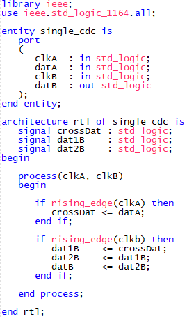
The VHDL code of this problematic design is the following:
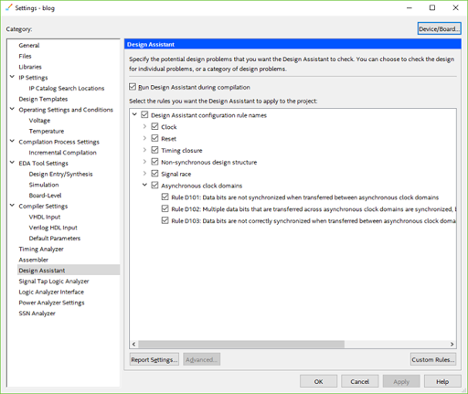
And if we try to run the Design Assistant of Quartus with the Asynchronous clock domains rules enabled
We get the following message:
Critical Warning (308060): (High) Rule D101: Data bits are not synchronized when transferred between asynchronous clock domains. (Value defined:2). Found 1 asynchronous clock domain interface structure(s) related to this rule.
The data could be lost for different reasons.
What happens if clkA is faster than clkB?
We can completely miss dataA and so the minimum pulse width of dataA must be 1.5 times the period of clkB. With three edges we have guarantee that the signal will be sampled at least once but this alone is not enough, we need additional flip-flop synchronizers to give more time to the metastable signal to settle.
Usually articles about CDC advise to use at least two flip-flops but as recommended by Altera, three flip-flop are a better solution given modern high-speed capable FPGA.
Below the VHDL code of this three flip-flop synchronizer:
But what to do if datA is a fast pulse that doesn’t meet the three edges of receiver rule?
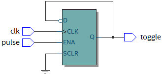
If pulses are anyway isolated enough we can convert pulses into toggles with this simple circuit.
Below the logic simulation of the circuit: every pulse sampled change the polarity of the toggle signal that, if pulses are far from each other, can (you need to do a little of math) meet the requirement of the minimum pulse width.
NB: The 2-XOR gate is also called programmable inverter because with one pin tied to HIGH the behavior is the same of an inverter while with one pin tied to LOW the signal on the other pin pass unchanged.
Quartus can furthermore optimize the design using one flip-flop with the Enable port. The behavior is the same and the pulse act as an Enable signal, as with the 2-XOR.
On the receiver side…
SORRY, CONTINUE TOMORROW
Disclaimer: This series of articles only scratch the surface of the topic. A very deeply paper about this topic is Clock Domain Crossing (CDC) Design & Verification Techniques Using SystemVerilog from Clifford E. Cummings and its reading is strongly suggested also if you don’t use SystemVerilog.


Nessun commento:
Posta un commento